Loading...
Searching...
No Matches
J7 — The QWA309 base board: hardware reference
- Variant
- mtb-mpy and mtb-only
This chapter applies to both packages. The hardware is the same, and the C code that reads the base board (proj_cm55/modules/cm55_sensor_poll/ and the GPIO & RGB Matrix page) ships as source in both.
What this chapter is for
This chapter is the hardware reference for the QWA309 base board under the AI Kit SoM: what each switch, knob and header is, which pin it reaches, and what firmware can and cannot read. The GPIO & RGB Matrix page is its on-screen companion; every switch and knob that page shows carries its pin beside it.
The pinout diagram
The diagram below puts every table of this chapter in one picture. For a sharp zoom, open the SVG version. Rows the diagram could not establish are the ones this chapter marks as not established.
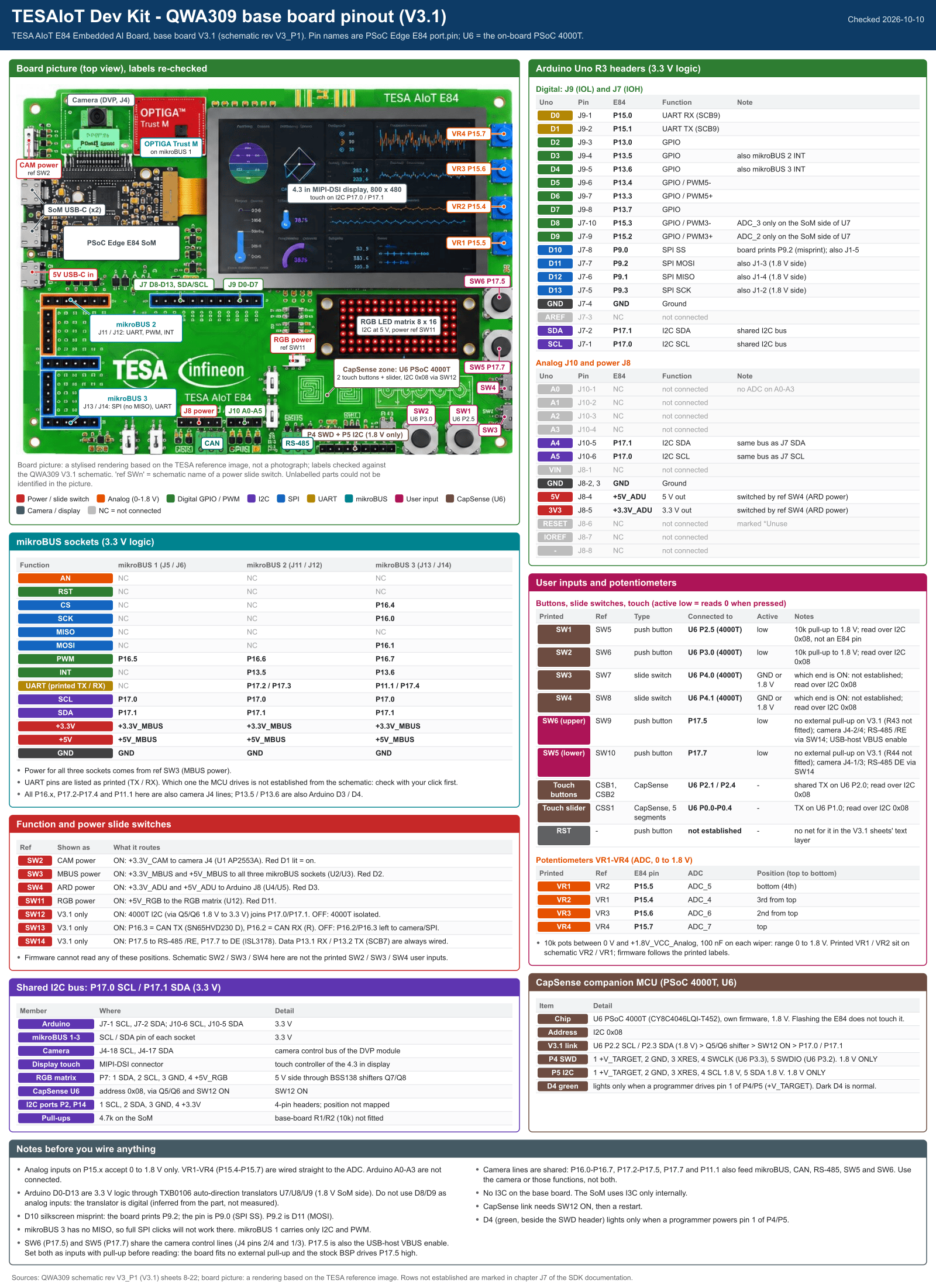
QWA309 base board pinout, V3.1
Every switch has two names
The board uses two naming systems at once: the printed label (the silkscreen) and the schematic reference designator (refdes). For the switches a user operates, the two never agree. This chapter always gives both, as in "printed SW1 (refdes SW5)".
The name SW3 means two different parts: printed SW3 is a slide switch the CapSense controller reads, while refdes SW3 is the mikroBUS power switch. When you read other documents or talk to other people, ask which naming they mean.
The two push-buttons on the E84 are SW6 (P17.5, upper) and SW5 (P17.7, lower). The pin is printed beside each button.
Inputs a user presses or slides
| Printed | Refdes | Kind | Wired to | How firmware reads it |
|---|---|---|---|---|
| SW1 | SW5 | push-button | CapSense controller pin P2.5 | only through the controller, and only when its firmware speaks protocol 0x0D or 0x0E |
| SW2 | SW6 | push-button | controller pin P3.0 | as above |
| SW3 | SW7 | slide switch | controller pin P4.0 | as above (ON/OFF) |
| SW4 | SW8 | slide switch | controller pin P4.1 | as above (ON/OFF) |
| SW5 | SW10 | push-button | E84 P17.7 | Cy_GPIO_Read() returns 0 while pressed |
| SW6 | SW9 | push-button | E84 P17.5 | Cy_GPIO_Read() returns 0 while pressed; read P17.5 and P17.7: shared pins, and one hazard first |
| BTN0, BTN1, slider | — | touch buttons and a touch slider | CapSense controller | through the controller, with either firmware |
SW1 to SW4 are not wired to the E84; no E84 pin can read them directly. Which way is ON for SW3 and SW4 cannot be read from the drawings: slide the switch and watch the GPIO & RGB Matrix page.
Potentiometers VR1 to VR4
| Printed | Pin | SAR channel | Refdes |
|---|---|---|---|
| VR1 | P15.5 | 5 | VR2 |
| VR2 | P15.4 | 4 | VR1 |
| VR3 | P15.6 | 6 | VR3 |
| VR4 | P15.7 | 7 | VR4 |
The pin printed beside each knob is right; only the VR1/VR2 numbers are swapped against the schematic designators. Firmware follows the printed labels (s_pot_adc_ch[] is { 5, 4, 6, 7 } in cm55_sensor_poll.c).
Each knob is a 10 kOhm potentiometer between the 1.8 V analog rail and GND, so its wiper swings 0 to 1800 mV, which the SAR reads as 0 to 4095. In millivolts that is raw * 1800 / 4095. The GPIO & RGB Matrix page shows both the mV value and the raw count.
Power and function switches
All of these are slide switches, and firmware cannot read their positions. Names in this table are refdes.
| Refdes | What it switches |
|---|---|
| SW2 | camera 3.3 V rail |
| SW3 | 3.3 V and 5 V rails of all three mikroBUS sockets |
| SW4 | 3.3 V and 5 V rails of the Arduino header |
| SW11 | RGB matrix 5 V rail |
| SW12 | ON: the CapSense controller joins the main I2C bus (P17.0/P17.1); OFF: isolated |
| SW13 | ON: P16.2/P16.3 go to the CAN transceiver; OFF: left to the camera or SPI |
| SW14 | ON: P17.5 drives the RS-485 transceiver's RE pin and P17.7 its DE pin |
The RS-485 data lines are always wired, not switched: the ISL3178's RO goes to P13.1 (SCB7 UART RX) and its DI comes from P13.2 (SCB7 UART TX). SW14 switches only RE and DE.
The CapSense controller
It is a second MCU. The CapSense controller is a PSoC 4000T (U6) on the base board, with its own firmware, running at 1.8 V. Flashing the E84 through KitProg3 never changes it; its only programming port is header P4 (SWD, 1.8 V only).
How the E84 reaches it. At I2C address 0x08 on P17.0/P17.1, with SW12 ON. The controller is also on header P5, a 1.8 V bus. Never connect a 3.3 V device to P5.
The green LED D4 next to P4 lights only when something plugged into P4 or P5 supplies about 1.8 V on pin 1, such as a programmer. Nothing on the board drives that pin, so a dark D4 is normal and does not mean the controller is unpowered.
What it sends. The controller runs one of two kinds of firmware:
- Legacy. The first three bytes are button 0, button 1 and the slider. It reports no SW1 to SW4 state.
- Snapshot, protocol 0x0D or 0x0E. The first six bytes are a marker byte 0xC5, the protocol number, a counter that advances with every update, a status byte, and the slider position as a 16-bit little-endian value (0 to 100, or 0xFFFF while nobody touches it).
The snapshot status byte:
| Bit | Meaning |
|---|---|
| 0x01 | BTN0 touched |
| 0x02 | SW1 pressed |
| 0x04 | SW2 pressed |
| 0x08 | SW3 in the ON position |
| 0x10 | SW4 in the ON position |
| 0x20 | BTN1 touched |
| 0x40 | the controller reports an error |
| 0x80 | the controller is running |
The controller debounces SW1 to SW4 before it reports them.
How the template reads it. Every 50 ms CM55 reads six bytes from 0x08 without writing a register address first (so the read starts at the start of the controller's buffer) and decodes either kind (cm55_capsense_frame.h): if the first two bytes are C5 0D or C5 0E it is a snapshot, otherwise legacy. SW1 to SW4 states are available only from a snapshot.
When CapSense shows nothing
The status line of the GPIO & RGB Matrix page tells you which case you are in:
- "no answer at 0x08" — the controller did not answer at start-up. Slide SW12 to ON and restart the board: firmware probes for the controller once, at start-up.
- "legacy 3-byte firmware" — touch buttons and slider work, but SW1 to SW4 need controller firmware protocol 0x0D or 0x0E.
- "protocol 0x0D" or "protocol 0x0E" — everything is available.
Reflashing the E84 cannot fix a problem in the controller. The other way round, changing the controller's firmware changes what the page shows even when the E84 still runs the same image.
The Arduino Uno header
The D numbers are the standard Arduino Uno positions; they are not printed on the board.
| Uno pin | E84 pin | Note |
|---|---|---|
| D0 | P15.0 | UART RX (SCB9) |
| D1 | P15.1 | UART TX |
| D2 | P13.0 | |
| D3 | P13.5 | shared with mikroBUS socket 2 INT |
| D4 | P13.6 | shared with mikroBUS socket 3 INT |
| D5 | P13.4 | PWM |
| D6 | P13.3 | PWM |
| D7 | P13.7 | |
| D8 | P15.3 | PWM or GPIO; not an analog input (see the note below) |
| D9 | P15.2 | PWM or GPIO; not an analog input (see the note below) |
| D10 | P9.0 | SPI SS; the board prints "P9.2", which is wrong |
| D11 | P9.2 | SPI MOSI |
| D12 | P9.1 | SPI MISO |
| D13 | P9.3 | SPI SCK |
| SDA / SCL | P17.1 / P17.0 | the main I2C bus |
- The header has no analog input. A0 to A3 are not wired (J10 pins 1 to 4). P15.2 and P15.3, which the E84's ADC can read, reach D9 and D8 through a TXB0106 level translator (U7), a digital part, so D8/D9 cannot be used as analog inputs. This is inferred from the part type, not measured. The base board's only analog inputs are the knobs VR1 to VR4.
- D0 to D13 are all 3.3 V logic through TXB0106 auto-direction translators (U7, U8, U9); the SoM side is 1.8 V.
- Header J1 (6-pin, 1.8 V SPI: 1.8 V, P9.3 SCK, P9.2 MOSI, P9.1 MISO, P9.0 SS, GND) sits on the SoM side of U7, so it shares P9 with D10 to D13.
- The header's 3.3 V and 5 V come through SW4; RST, AREF, VIN and IOREF are not connected.
The three mikroBUS sockets
| Pin | Socket 1 | Socket 2 | Socket 3 |
|---|---|---|---|
| AN, RST | not connected | not connected | not connected |
| CS | not connected | not connected | P16.4 |
| SCK | not connected | not connected | P16.0 |
| MISO | not connected | not connected | not connected |
| MOSI | not connected | not connected | P16.1 |
| PWM | P16.5 | P16.6 | P16.7 |
| INT | not connected | P13.5 | P13.6 |
| TX | not connected | P17.2 | P11.1 |
| RX | not connected | P17.3 | P17.4 |
| SCL / SDA | P17.0 / P17.1 | P17.0 / P17.1 | P17.0 / P17.1 |
- Socket 3 has no MISO, so a Click board that reads data back over SPI does not work there without hand wiring.
- The TX/RX rows for sockets 2 and 3 follow the silkscreen, but the schematic net names suggest the opposite direction; which is right is not established for either socket. Check before relying on UART in socket 2 or socket 3.
- All three sockets take power through SW3. Every P16.x pin, P17.2 to P17.4 and P11.1 are also DVP camera lines.
I2C and I3C
The base board has no I3C: no schematic sheet carries an I3C net. The I3C you may see in other documents belongs to the SoM, which uses it internally for the BMM350. The header printed "I2C 1.8V ONLY" is P5, the CapSense controller's own bus. The main 3.3 V bus (P17.0/P17.1) uses the pull-ups on the SoM; the base board's own pull-ups (R1/R2) are not fitted. The bus is also brought out on two 4-pin I2C ports, P2 and P14 (1 SCL, 2 SDA, 3 GND, 4 3.3 V); where they sit on the board is not established.
P17.5 and P17.7: shared pins, and one hazard
| Pin | Shared with |
|---|---|
| P17.5 | push-button SW6 · camera line on J4 (base-board net PEN; the SoM BSP calls it camera reset) · RS-485 RE through SW14 · USB-host VBUS enable |
| P17.7 | push-button SW5 · camera line on J4 (net PDN; the BSP calls it camera power-down) · RS-485 DE through SW14 |
The camera module and its power switch (SW2) can load these lines; their effect on reading the buttons has not been measured.
- Warning
- Do not press the P17.5 button before the GPIO & RGB Matrix page has been opened. At boot the BSP configures P17.5 as a strong output driven high (it is the camera reset line and the USB-host VBUS enable). The button on P17.5 connects that pin straight to GND with no series resistor, so pressing it before firmware reconfigures the pin shorts a driven-high output to ground for as long as the button is held. The GPIO & RGB Matrix page reconfigures P17.5 as an input with a pull-up the first time it opens. No damage has been seen, but this is not a measured limit. The P17.7 button carries no such risk: P17.7 is driven low.
The USB-host VBUS enable shares P17.5 with this button. The GPIO & RGB Matrix page reconfigures P17.5 as an input.
The old pinout picture is not a source
The older pinout picture that circulates with the board (marked Version 3.1, not the diagram in this chapter) contradicts the schematic in four places: it shows A0 to A3 on P15.2 to P15.5 (they are not wired), VR1 on P15.2, the SW5/SW6 buttons on "P8.x", and D0 as P9.0 (it is P15.0). Use this chapter or the schematic instead.
Reading the base board from C
Everything below runs on CM55, called from the GFX task (the task LVGL runs in), which is what the GPIO & RGB Matrix page (page_gpio_rgb.c) does.
- Knobs. cm55_pot_read_all(uint16_t out[4]) returns raw 0 to 4095 in printed order (VR1 to VR4), and returns 0 until the SAR is ready.
- Buttons on P17.5/P17.7. Configure the pin with Cy_GPIO_Pin_FastInit(port, pin, CY_GPIO_DM_PULLUP, 1, HSIOM_SEL_GPIO); Cy_GPIO_Read() then returns 0 while the button is pressed.
- CapSense. cm55_capsense_info() (cm55_sensor_poll.h) says whether the controller answers, which protocol it speaks, and the SW1 to SW4 states when it has them. BTN0, BTN1 and the slider arrive in the sensor-hub snapshot (ipc_sensor_capsense_t, whose layout is unchanged), and CM33 reads the same values through the cm55_controls_snapshot hook.